
How does RRP Electronics' new facility expand India's semiconductor packaging capabilities?
RRP Electronics inaugurated an Advanced Wafer-Level Packaging facility in Navi Mumbai on October 12, 2026, adding production for SIM and eSIM modules to its outsourced semiconductor assembly and test operations.
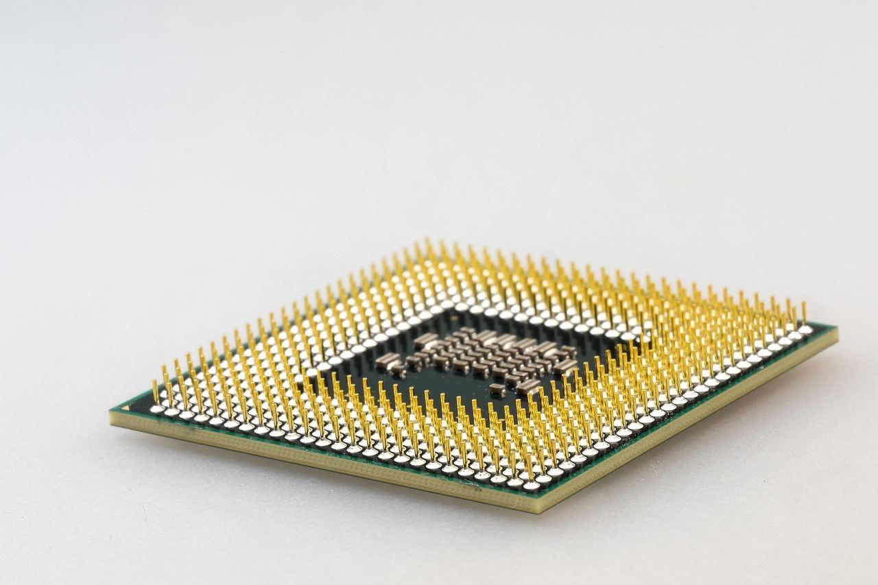
RRP Electronics Launches Advanced Wafer-Level Packaging Facility
On October 12, 2026, India's RRP Electronics officially opened an Advanced Wafer-Level Packaging (AWLP) facility within its semiconductor division in Navi Mumbai, Maharashtra. This new installation is designed to augment the company's existing outsourced semiconductor assembly and test (OSAT) services.
The inauguration marks a tangible expansion of RRP Electronics' operational footprint and technological offerings in the region, focusing on advanced processes crucial for modern electronic components. The facility's establishment reflects ongoing efforts by companies in Asia to enhance domestic capabilities across the semiconductor value chain.
Expanded Production for SIM and eSIM Modules
The newly operational AWLP facility is specifically equipped to produce Subscriber Identity Module (SIM) and embedded SIM (eSIM) modules. This specialisation positions RRP Electronics to cater to the increasing demand for secure and compact connectivity solutions across various devices, from consumer electronics to industrial internet-of-things (IoT) applications.
Beyond module production, the Navi Mumbai unit also integrates specialised testing procedures, ensuring the quality and reliability of the packaged semiconductors. This addition broadens the scope of services RRP Electronics can offer to its clients, moving beyond basic assembly to more complex, integrated solutions.
Enhancing India's Semiconductor Ecosystem
The launch of RRP Electronics' advanced packaging facility contributes to the development of India's domestic semiconductor ecosystem. As global supply chains continue to evolve, countries are prioritising the establishment of local manufacturing and packaging capabilities to reduce reliance on external markets and enhance resilience.
This investment by RRP Electronics aligns with broader national objectives to attract and cultivate semiconductor manufacturing and related services within India. The facility's focus on advanced wafer-level packaging, a critical step in semiconductor production, represents a move towards higher-value activities in the country's technology sector.
Implications for Regional OSAT Services
The new facility in Navi Mumbai represents a concrete expansion of India's domestic semiconductor manufacturing capabilities. For companies operating in the broader Asian electronics supply chain, this addition by RRP Electronics offers an expanded option for outsourced semiconductor assembly and test services, particularly for specialised module integration.
Investors tracking the growth of India's technology sector will observe further announcements regarding capacity utilisation and potential partnerships, with future Q4 2026 and H1 2027 company filings providing initial indicators of market uptake in this new segment.
This analysis is journalism, not investment advice; consult a licensed professional before making financial decisions.
Pieces are credited to the desk that commissioned and edited them. Our editorial standards, and the desks behind them, are set out on the Editorial Standards and Team pages.
Further reading
- Briefings · Markets
How do offshore NDFs transmit exchange rate pressure to Asia's markets?
A new BIS study reveals that a US$1 billion increase in offshore dollar demand can depreciate domestic spot rates by 10 basis points in minutes, widening offshore-onshore spreads.
Continue reading → - Briefings · Policy
How will MDBs deliver more financing for developing economies?
Heads of multilateral development banks met in Manila on 17 October 2026, affirming joint action to address challenges like economic uncertainty and high debt for developing nations.
Continue reading → - Briefings · Markets
Has SGX's 10-Share Lot Policy Diversified Market Activity?
Despite the Singapore Exchange's introduction of 10-share trading lots on October 5, 2026, market activity remains concentrated, with three local banks comprising a third of September's turnover.
Continue reading →